Week 6: Electronics Design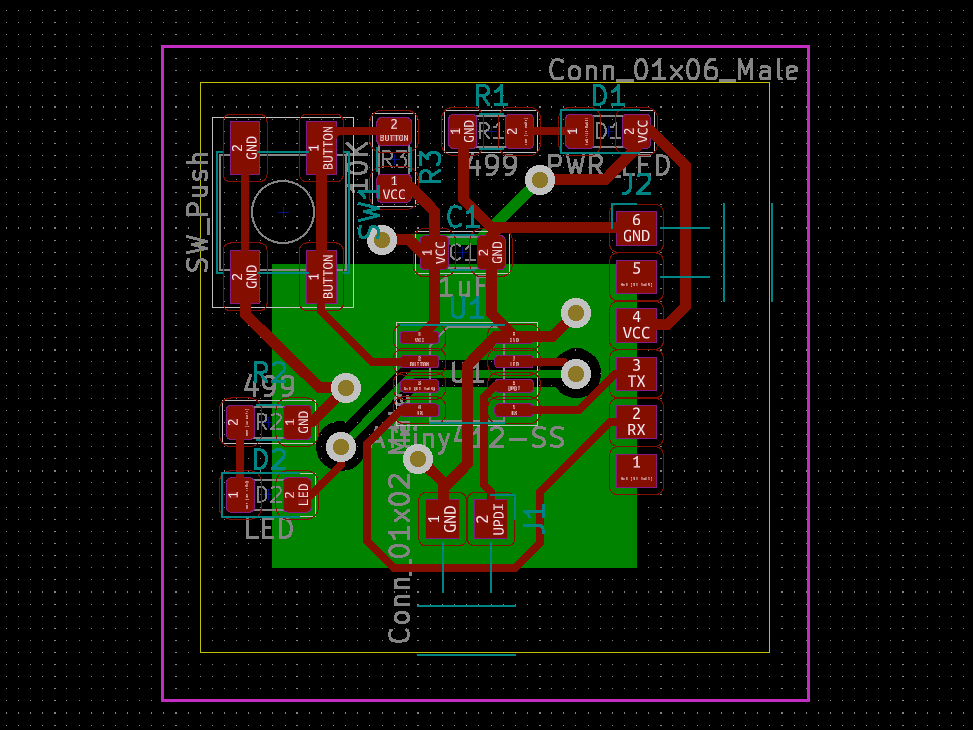
#KiCad #mods #PCB Milling #SMD Soldering
Assignments: (Group) 1. Use the test equipment in your lab to observe the operation of a microcontroller circuit board. (Individual) 2. Redraw an echo hello-world board, add (at least) a button and LED (with current-limiting resistor), check the design rules, make it, and test it, extra credit: simulate its operation.
Published on: Mar 04, 2020Last updated on: Jan 12, 2021
-
Individual Assignment: PCB Design Project - ATtiny 412 Double-Sided Board
- Materials
- Schematic Design
- Decide the Current-Limiting Resistor for LED
- ATtiny 412 Pins
- Annotate Schematic Symbols
- Assign Footprint
- Generate Netlist
- Complete Schematic
- Footprint Layout
- Import Netlist File
- Separate Layers
- Complete PCB View & Final Check
- Export PCB SVG
- Fill Holes with Vias to Connect Both Sides
- Solder PCB with Flux
Individual Assignment: PCB Design Project - ATtiny 412 Double-Sided Board

Materials
| # | Digi-Key Part No. | Name | Value * Pieces | KiCad Footprint(Package) |
|---|---|---|---|---|
| 1 | ATtiny 412-SSFRCT-ND | ATtiny 412 w/ Single-pin UPDI (Datasheet) | tinyAVR™ 1 Microcontroller IC 8-Bit 20MHz 4KB FLASH 8-SOIC * 1 | Package_SO: SOIC-8_3.9x4.9mm_P1.27mm |
| 2 | B3SN-3112P | B3SN Tactile Switch, SMD | * 1 | self-designed footprint: TACTILE_SW_B3S |
| 3 |
|
LED 1206 SMD |
|
LED_SMD: LED_1206_3216Metric_Pad1.42x1.75mm_HandSolder |
| 4 |
|
RES SMD 1% 1/4W 1206 |
|
Resistor_SMD: R_1206_3216Metric_Pad1.42x1.75mm_HandSolder |
| 5 | 445-1423-1-ND | CAP CER 1UF 50V X7R 1206 | 1 uF * 1 | Capacitor_SMD: C_1206_3216Metric_Pad1.42x1.75mm_HandSolder |
| 6 | 445-1423-1-ND | Male 1 Row Horizontal SMD Header 2.54MM |
|
self-designed footprint:
|
Design Tool: KiCad EDA
KiCad EDA is a cross platform and open source electronics design automation suite with lots of predefined symbol and footprint libraries provided by industrial companies such as Digi-Key and Teensy. I used it to design my PCB by redrawing the original hello.t412.echo board and adding two extra LEDS (a power LED and a programmable LED) as well as a push-button.
Original hello.t412.echo Board

My Board

Schematic Design

Since I added the following components to my new board, it is common to add an extra resistor between the I/O pin of the ATtiny 412 chip or Vcc (input power) and the component itself to make sure that the current is not too high to break them:
- Power LED
- Programmable LED
- Push-Button

Decide the Current-Limiting Resistor for LED

There are two main rules which I learnt from Adafruit's Forward Voltage and KVL article to follow in order to design the correct circuit for the LED connection:
- Kirchhoff's Voltage Law (KVL): In any loop of a circuit, the voltages must balance, that is the amount generated = the amount used
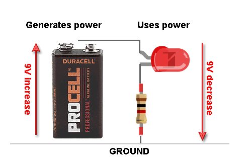
- Ohm's Law: V = I * R (V: voltage, R: resistance, I: current)
First, I tried to find the forward voltage of the LED I used from its datasheet which indicates that its forward voltage (VF) and forward current (IF) are around 3V and 20mA respectively, which means that I need to make sure that the cross-voltage of the LED cannot exceed 3.8V or it will burn down the LED.
In other words, the resistor used to limit the current to 20mA should consume the remaining 2V (Vcc - VF, Vcc =5V from USB, VF=3V). Then, I put these values (Vcc=5V, VF=3V, IF=20mA) into the equation to get the correct resistance:
Voltage across a resistor (V, volts) = Current through the resistor (A, amperes) * The Resistance of the resistor (Ω, ohms)
→ Vcc - VF = IF * R
→ 5V - 3V = 0.02A (= 20mA) * R
→ R = 100 Ω (the minimum value)

According the answer, I chose 499Ω which is above the 100Ω (the minimum value) as the resistance to form the circuit for both the power LED and the programmable one.

ATtiny 412 Pins
In order to program the self-designed board, I need to understand the function of each pin of the ATtiny 412 chip. Since ATtiny 412 has an Unified Program Debug Interface (UPDI) pin which is PA0 pin, it is easier to program it with a 1x2 male pin header (J1: Conn_01x02_Male).
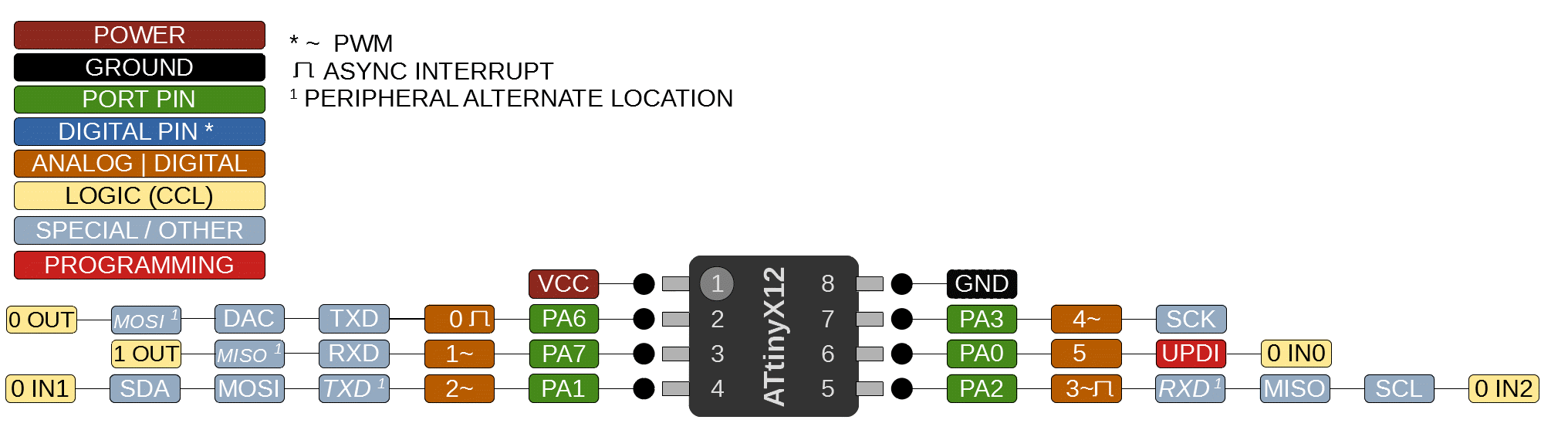
The other 1x6 male pin header (J2: Conn_01x06_Male) is connected to a FTDI cable or FTDI programmer board to power on and read data from the ATtiny 412 board by communicating through RX (PA1) and TX (PA2) pins.

For the other three remaining port pins, I used two of them as IO pins to control the programmable LED (PA3) and the push-button (PA6) respectively. Since I am not going to use PA7 and the other two pins of the FTDI male connector, I placed a no connection flag to it to make sure it does not work against the electrical rules while I check the performance by clicking

Besides, it is also a good habit to put a bypass capacitor between Vcc and GND pins (power pins) of the chip.

Annotate Schematic Symbols
In order to specify different components, I then opend the Annotate Schematic dialogue by clicking


Assign Footprint
Before layouting the printed circuit board, I need to assign which footprint belongs to which symbol (component) in the Assign Footprint dialogue by clicking


The name of each correspondent footprint is also arrranged in the material table shown on top of the page.
Generate Netlist
The final step of the schematic design is to generate the netlist file which will then be imported to the PCB layout mode. I did this by clicking


Complete Schematic

Footprint Layout
After finishing the schematic design, I then switched to the PCB layout mode via


Import Netlist File
In the PCB mode, I clicked

These are some messy nets which I am going to layout:


Define Trace Clearance, Trace Width & Via Size
Before starting to connecting components with traces, I clicked Board setup button

-
Clearance
- For normal traces which can be milled with 0.4mm bits: 0.4mm
- For tiny traces (e.g., smaller SMD chips) which can only be milled with 0.3mm bits: 0.3mm
-
Track Width
- For Default traces: 0.4mm or 0.3mm
- For Power traces (e.g., Vcc and GND): 0.6mm or more
- Via Drill: 0.8mm (depending on the size of copper hollow rivets introduced below)

Extra: THT (Through-hole technology) Components Setting
In order to mill THT components, I need to first adjust the hole size of certain components in the footprint library by clicking Open footprint editor button


I double clicked its pin holes to open Pad Properties dialogue, typed the correspondent size (here, 1.5mm for Hole size X) and made sure that the pad size of this hole is big enough for soldering by adjusting Size X and Y.

Separate Layers
After layouting all the components, I started to create traces between them by using

If there is not enough space for routing tracks, I then created vias which are conductive holes by using


Since there are many pins connect to GND, it is also useful to create a ground plane on the other side by switching to B.Cu layer and using


The final step of the PCB layout is to define its outline for mods to generate its interior toolpath. To do that, I first switched to the Edge.Cuts layer and used


Finally, I added a pink rectangular outline to the Margin layer which is reserved for the drawing of circuit board outline. Any element (graphic, texts…) placed on this layer appears on all the other layers. It also defines the board area for exporting the image for each layer.
Complete PCB View & Final Check
Below I listed some notes according to different layers:
-
Edge.Cuts layer: yellow outline
- every component (including gray texts and green footprints) should be inside this layer.
-
Dwgs.User layer: gray fill
- the size of this layer should be the same as Edge.Cuts layer.
-
Margin layer: pink outline
- make sure there is no gray texts in this layer, otherwise there will be some flipping problems during milling.
- make sure the left and right margins are even by specifically defining the coordinates of two vertical lines along x-axis in Line Segment Properties dialogue.

Export PCB SVG
Before starting milling the board, we need to generate the image files for its front-side traces, back-side traces, drilling and outline. I did this with the following steps and settings:


For the drilling svg, I filtered out the vias from the F.Cu.svg and infilled them with black color in Inkscape:

Fabrication: SRM-20 Milling Machine
The fabrication of the PCB is almost the same as the process of Week 4: Electronics Production except the server module used to generate the cutting toolpath in mods is:
p.s. MDX-40 milling machine uses the follwing same svg mods server module.

mods Toolpath Setting Comparison (MDX-40)
Link to tutorial of MDX-40 milling machine
- origin: (x, y, z) = (0, 0, 0) mm
- home: (x, y, z) = (0, 0, 5) mm
| tool diameter | cut depth | max depth | offset number | speed | color |
|---|---|---|---|---|---|
| 0.3mm | 0.125mm | 0.125mm | 4 | 1.0mm/s |
|
| 0.4mm | 0.125mm | 0.125mm | 4 | 1.5mm/s |
|
| 0.8mm (Outline) | 0.6mm | 1.8mm | 1 | 2.0mm/s |
|
| 0.73mm (Drill) | 0.6mm | 1.8mm | 1 | 2.0mm/s |
|
Front Side: F_Cu.svg (0.3mm), F_Drills.svg & Dwgs_User.svg (0.8mm)

Back Side: B_Cu.svg (0.4mm)

Fill Holes with Vias to Connect Both Sides
Before soldering the PCB, I first inserted the copper hollow rivets


Solder PCB with Flux
It is also beneficial to use a liquid flux pen to put some flux on the board before soldering any SMD components.

End Result
The board I redrew finally works after I programmed it. The ATtiny 412 programming process and the setup environment will be introduced in Week 8: Embedded Programming.
Blink the LED
Problem & Solution
The inital connection of the switch I designed was wrong, which I found out after uploading the code to the board. It lacked a 10kΩ resistor as a pull-up or pull-down resistor whose function can be found from the Sparkfun: Pull-up Resistors article. Since it takes quite a long time to reconstruct a new board, I then decided to solder a through-hole resistor to fix the problem.


It works after I reuploaded the code.
LED OFF

Press the button to light up LED

Group Assignment: Debugging & Measurement
Link to Documentation Page
Debugging Tool: Multimeter
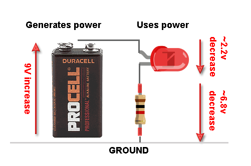
After finishing soldering, I used a multimeter and switched it to the buzzing mode which sounds if two points are connected (0Ω between them). In order to find out how much current does each LED consume, I then measured their cross voltage by switching to the DC voltage mode:
Measure the Connection
Measure the Cross Voltage
The red dots between each component are multimeter probes. According to the statistic, I can calculate the exact current which go through both the LED and the resistor:
Voltage across a resistor (V, volts) = Current through the resistor (A, amperes) * The Resistance of the resistor (Ω, ohms)
→ Vcc - VF = IF * R
→ VR = IF * R
→ 2.148V = IF * 499 Ω
→ IF = 0.0043A = 4.3mA
VF: Cross Voltage of Power LED


VR: Cross Voltage of Resistor


Then I used the multimeter to verify my calculation and it seems that there is some difference between the theoretical number and the practical one when it comes to measuring small current which can be observed by an oscilloscope in a more precise way:
LED OFF

LED ON

